 English
 Russia
 Hecheng Electronic Technology Group Limited

Product Detail:
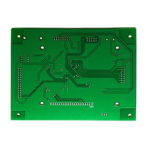
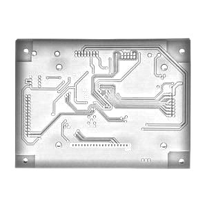
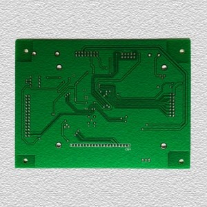
2 layer PCB has more layers than a 1-layer PCB, but less than a multilayer PCB. 2 layer PCB can install conductive copper and components on both sides of the printed circuit board so that the traces can cross each other. Therefore, a higher density circuit board can be realized without point-to-point soldering. It is therefore difficult to manufacture 2-layer PCBs because they are more complex than 1 layer PCBs. However, it is better to use 2-layer PCB than 1 layer PCB. 
Hecheng Fast Electronic Technology was established in the year 2009 in SHENZHEN as Printed circuit board manufacturers. Over the years we have grown by leaps and bounds in the field of printed circuit boards. We can supply complete array of PCB products to meet your customized requirement. Our product range includes single sided, double sided, multi-layer, metal clad PCB.
The production of double-sided panels is more complicated than single-sided panels. The main reasons are as follows:
(1) The top and bottom layers of the copper clad laminate/laminate must be laid out
(2) The top and bottom circuits should be connected to PTH.
One of the most critical is PTH, which is also the core process of double panel production. The so-called PTH is produced by plating/plating a layer of metal on the inner wall of the through hole to connect the top and bottom printed circuits. At present, the domestic PTH mainly adopts the electroless copper plating process. There are two kinds of electroless copper plating process:
①The thin copper is electrolessly plated first, then the whole plate is electroplated to thicken the copper layer, and finally the pattern transfer is carried out.
②The thick copper is electrolessly plated first, and then the pattern is directly transferred.
Both of these processes are widely used. However, the electroless copper plating method is harmful to the environment and will gradually be replaced by more advanced black hole technology, tin/palladium direct electroplating technology, and polymer direct electroplating technology.


