 Hecheng Electronic Technology Group Limited

As we know, PCBs basically interconnect the electronic components by creating conductive pathways via copper pads and connecting lines. Therefore, the PCB assembly process becomes one of the most intriguing concepts in electronics. Today PCBearth.com will talk about the PCB assembly process.

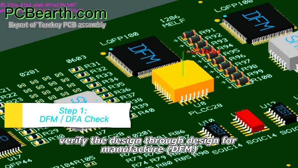
Step 1: DFM / DFA Check
Once a PCBA order is placed to PCBearth's production team, their first task is to verify the design through a thorough DFM/DFA check process. These checks include verifying the consistency of different design documents (BOM, Gerbers, Centroid, etc.), part spacing, footprint accuracy, and clear direction markings.
Step 2: Material Inspection
When the components are received at PCBearth's production facility, our incoming quality control (IQC) team will conduct a thorough inspection before entering any specific materials or components. Inspection includes sample operation test and date code verification and access to the software material management system. We ensure that the parts used in PCB assembly are always in good working condition.
Step 3: Print Solder Paste on the PCBs
The first step in the actual PCB assembly process is to apply solder paste on the bare PCB. Here, the stainless steel template created during the PCB manufacturing process is mounted on the bare board, leaving only the pads used to assemble the surface mount components uncovered. The template is held in place by a mechanical fixture, and the applicator is moved on the surface of the circuit board to carefully distribute the solder paste on those uncovered spaces. Our quality control team conducts thorough inspections to ensure that solder is only applied to the necessary areas and all pads are covered with a sufficient amount of solder paste.
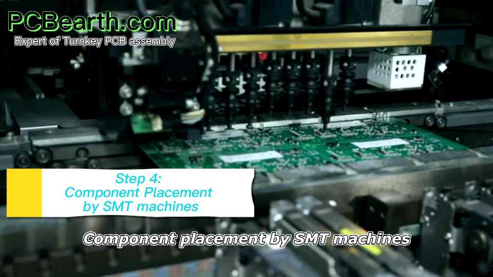
Step 4: Component Placement by SMT machines
Once the solder paste is applied to the bare PCB, they are transferred to the automatic pick and place machine to actually mount the components on the relevant pads. Part placement is 100% machine automation to achieve maximum accuracy and efficiency, and the project's centroid file is used to obtain component coordinates and rotation data. Check the circuit board again after installing the components to ensure that all placements are accurate before the soldering process begins.
Step 5: Over Reflow soldering
With parts mounted securely in place with solder paste underneath their pads, it is time for the PCB to enter the reflow soldering stage. This is the most commonly used PCB assembly method in the industry today because it is more flexible in terms of PCB layout requirements than wave soldering or manual soldering. In most cases, we can use reflow soldering for most of the components on the board, and then hand over most of the assembled circuit boards to our skilled manual soldering team to make the last few connectors.
Step 6: Inspection after SMT
After the reflow cycle, any boards including BGA, QFN or other lead-free package types are sent for X-ray inspection. X-rays penetrate the silicon of the IC package and reflect from the metal joints below, forming an image of the solder joint itself, which can be analyzed by advanced image processing software similar to automatic optical inspection (AOI). The higher density of features in the capture area will produce a darker result image, allowing quantitative analysis to determine the quality of the solder joint and compare it to industry standards.
X-ray inspection can not only detect problems in PCB assembly, but the analysis of X-ray images can help determine the root cause of a given defect, such as insufficient solder paste, skewed component placement, or improper reflow profile.
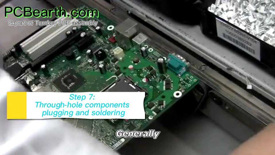
Step 7: Through-hole components plugging and soldering
The board also may contain a number of through-hole components, in which case these components require a special kind of soldering method. This could be manual soldering where components will be inserted one at a time. The process can be lengthy depending on how many components there are. There is also wave soldering which is an automated version. Wave soldering is a method of PCB Assembly that involves sending boards on a conveyor through a “wave” of molten solder. The solder bonds together exposed component pads and leads while wicking off of the bodies of components and the solder masked bulk of the board.
Step 8: Final inspection, cleaning and packing.
Inspections are performed after each individual stage of the PCB assembly process to better locate the source of any errors. We believe that these intermediate inspections are necessary, but not enough to fully guarantee the highest process quality. This is our mission, so we always perform a thorough final inspection of the fully completed circuit board at the end of the process. Afterwards, we will clean with deionized water, because welding will leave some residue. After washing, it is dried under compressed air and packed fine products.

PCBearth provides professional PCB assembly services. Over the years, we have improved our processes to ensure that our customers get the best value in every project. The cooperation with PCBearth gives you complete confidence that your PCB project will be carried out with the best quality control, efficiency, flexibility and customer service.
We can handle designs and requirements of all types, and we encourage prospective clients to get in touch with us for any questions that might not be captured in this brief overview. You can contact us by email.