 Hecheng Electronic Technology Group Limited


Product Detail:
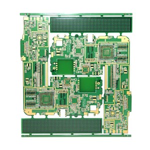
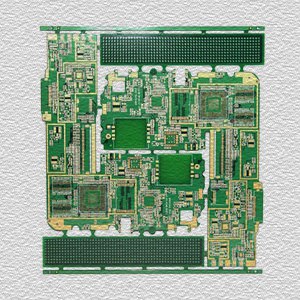
Multilayer PCB refers to a printed circuit board with more than two copper layers, such as 4L, 6L, 8L, 10L, 12L, etc. As technology advances, people can place more and more copper layers on the same board. Currently, we can produce 20L-32L FR4 PCB.
Through this structure, engineers can place traces on different layers according to different purposes, such as power layer, signal transmission layer, EMI shielding layer, component assembly layer, etc. In order to avoid too many layers, a Buried Via or Blind Via is designed in a multilayer PCB. For boards with more than 8 layers, high TG FR4 materials will be more popular than ordinary TG FR4.
The more layers, the more complicated and difficult it is to manufacture, and the more expensive it is. The delivery time of multi-layer PCB is different from ordinary PCB, please contact us for the exact delivery time.
Hecheng Fast Electronic Technology is a trustworthy company that provides the best circuit boards for advanced electronic products. We focus on the design and production of multilayer printed circuit boards. If you need to get your PCB as soon as possible, you can trust Hecheng Fast Electronic Technology.
Our well-trained assembly technicians specialize in multilayer circuit boards. They use the most advanced multilayer circuit board manufacturing equipment to ensure that the finished boards we distribute meet your strict standards and technical specifications. You will also find that our multi-layer PCB prices fit your project budget.
The general structure of the multilayer board is as follows:
Top silkscreen: Identify the name, board number, data, etc. of each PAD;
Finishing of the top surface: protect the bare copper from being oxidized;
Top Soldermask: Protect copper from being oxidized and not being soldered during SMT;
Top Trace: Copper is etched to perform different functions according to the design
Substrate/core material: non-conductive, such as FR4, FR5
Prepreg (PP)
Intermediate layers, such as GND, VCC, Inner 3, Inner 4, etc.
Prepreg (PP)
Bottom traces: (same as above)
Bottom solder mask: (same as above)
Finishing of the bottom surface: (same as above)
Bottom silkscreen/Legend: (same as above)


