 Hecheng Electronic Technology Group Limited

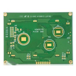
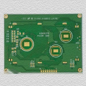
Product Detail:
High layer count PCBs, widely found in file servers, data storage, GPS technology, satellite systems, weather analysis and medical equipment are usually ≥12L with special performance requirement raw material.
Specific high-tech PCB attributes that affect delivery time: 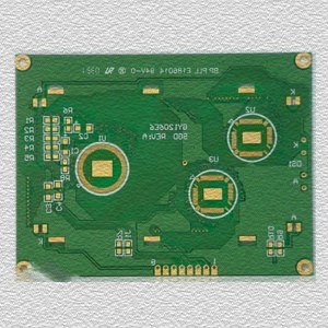
Via-In pad technology
As the level of technology improves over time, in-pad via technology has become very common in PCBs. Many people don't realize how this technology is made and how long it will take. The design of the via in the pad means that we will drill a via (VIA) in the pad and then fill the via with a conductive epoxy filler. The process of filling the through-holes will increase the manufacturing process by more than 8 hours, because the material needs to be heated to a certain temperature before filling the through-holes, and then it needs to be cured through a long post-process.
Designated dielectric
Many PCB designers try to specify the dielectric thickness of a layer to obtain the specific impedance value they need for their design. As a PCB manufacturer, it will be easier for us if we can use the combination of dielectric thickness and line width adjustment to obtain the required impedance. This is because most manufacturers use different common stacks based on their customer base and product mix. This means that if you specify a controlled impedance value, you need to let your PCB manufacturer determine the best stack to achieve your goal, so you can save time and money.
Buried hole
When the vias are buried in the inner layer, each group requires a separate lamination cycle, which requires the entire stack to process 50% of each group of buried holes. On the other hand, the blind holes connecting the outer layer and the inner layer do not require so much additional processing. For blind holes, if most PCB manufacturers invest in laser drilling, they will use laser drilling to control the depth of the blind holes before plating all through holes.
Conductive filled vias
You can see more details in the vias in the pads, but many designs require this technique to dissipate heat from the component. One of the biggest failures of filling through holes is that they did not take enough processing time to properly cure the solder paste in the very small holes, and customers only saw voids and outgassing on the printed circuit board when they were assembled and started to use.


